AT-RISC Registers
Table of Contents
Registers
Let us take a look at the register file now.
As mentioned in my motivations, I want this design to closely follow RISC-V style, however I do not want it to be identical.
In the RV32I Specification RISC-V is designed with 32 General purpose registers. Using TTL hardware this is insane at an 8-bit level, let alone a 16-bit level.
| Register Count | 8-Bit | 16-Bit |
|---|---|---|
| 4 Registers | 12 | 24 |
| 8 Registers | 24 | 48 |
| 16 Registers | 48 | 96 |
| 32 Registers | 96 | 192 |
This table shows how many chips would be required, under my current design, for $n$ registers and $m$ word size, just for data storage and bus driving.
I think, a healthy balance between processing power and practicality will be starting with 8 16-bit registers, this can be represented in a 3-bit address, I will however reserve 1 extra bit to allow myself the option to double this up to 16 registers at a later date. These registers will be labelled $r0$ through to $r7$, much like the RISC-V specification, $r0$ will be a hardwired zero register.
Verilog Implementation
The register file will hold and control all the individual registers, it will have 7 main inputs and outputs
Inputs
| Name | Width | Purpose |
|---|---|---|
| A1 | 3/4 | Address for Read Data 1 (RD1) |
| A2 | 3/4 | Address for Read Data 2 (RD2) |
| A3 | 3/4 | Address for Write Data |
| WE | 1 | Write Signal |
| WD | 16 | 16-Bit data to write to address A3 |
Outputs
| Name | Width | Purpose |
|---|---|---|
| RD1 | 16 | Read Data 1 (RD1) |
| RD2 | 16 | Read Data 2 (RD2) |
As you can see by these inputs and outputs, we follow the “LHS” and “RHS” style design, where instead of hardcoded left and right registers, we can select any one.
Verilog Register
The Verilog code is reasonably straightforward, if anything I am massively overcomplicating it by adding a register module instead of initialising a 7, 16-bit registers in the register file Verilog.
module register (
    input CLK,
    input WE,
    input [15:0] WD,

    output [15:0] RD
);

    reg [15:0] data;
    initial data = 16'b0;

    always @(posedge CLK) begin
        if (WE)
            data <= WD;
    end

    assign RD = data;

endmodule
I also wrote some tests for this, I won’t include them in the text body but they will be uploaded to the repository along with the source.
Register File
Once again I am providing reasonably straight forward code for the registerfile. In these code blocks the register module is always outputting to RD, and the registerfile module chooses which one drives RD1 and RD2.
module registerfile (
    input CLK,
    input [2:0] A1, A2, A3,
    input WE,
    input [15:0] WD,

    output [15:0] RD1, RD2
);

    // Outputs from registers
    wire [15:0] reg_out [7:0];

    // Write enable decoder
    wire [7:0] we_decoded;
    assign we_decoded = WE ? (1 << A3) : 8'b0;

    // Always outputs 0
    assign reg_out[0] = 16'b0;

    genvar i;
    generate
        for (i = 1; i < 8; i = i + 1) begin : regs
            register r (
                .CLK(CLK),
                .WE(we_decoded[i]),
                .WD(WD),
                .RD(reg_out[i])
            );
        end
    endgenerate

    assign RD1 = reg_out[A1];
    assign RD2 = reg_out[A2];

endmodule
Once again, there are some tests on the GitHub repository for this project.
Physical Implementation
Breadboard
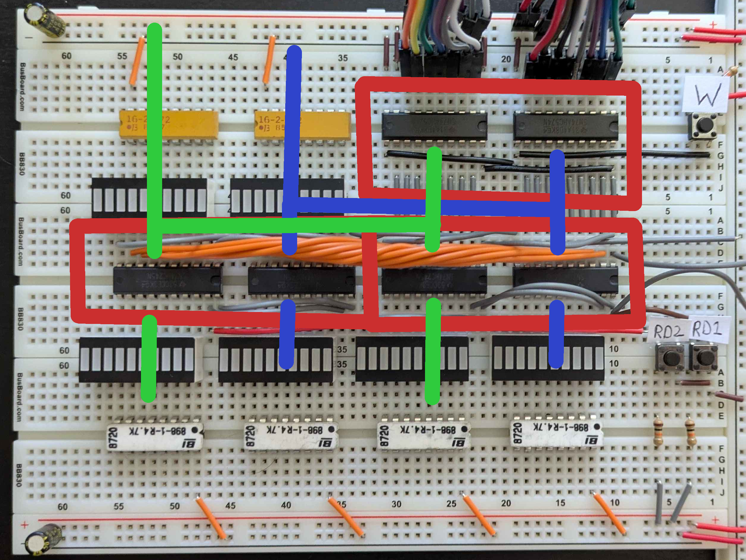
I have physically implemented one of the registers on breadboard, Implementing more than one would involve an impractical amount of wiring.
This module contains:
2 x 74HC574 Octal Flip Flops
- These actually store the data and is triggered by a write pulse.
4 x 74HC245 Tri-State Octal Transceivers
- These are split into two 16-Bit transceiver blocks, with one to drive RD1 and the other to drive RD2.
Write Button
RD1 & RD2 Out Button
LED output
- Only the flip flop side LEDs will be present on a final build, the lower ones are purely for showing the outputs
It is also fun to note the resistor networks which are actually older than me!
Schematic
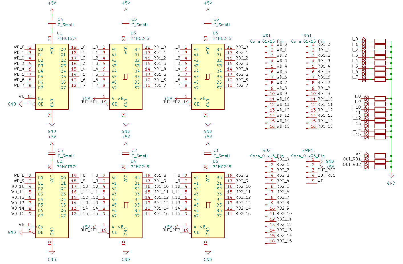
The schematic is pretty much the same as the breadboard version. The only difference is no output LEDs and the presence of signal LEDs for enabling of writing and output.
Discussion
In my research I considered replacing the 8-bit chips with 16-bit equivalents. Such as the 74HC16541 and the 74HC16374, however the cost difference and smaller package sizes don’t seem worth it to me.
I have also considered, and possibly still will, switch to the one way equivalent of the 74HC245, the 74HC244. This would be very simple to switch to, it just depends on if there is a price difference when sourcing the components.
I haven’t full fleshed out the design for the zero register and address decoder yet, however I am reasonably confident it will use 74HC238s as the decoders, and ideally keep the zero register and decoder on the same board so a 8 register file will contain 8 evenly sized and spaced registers.
That’s it for this post, I’m very much enjoying this project and can’t wait to see where it will take me. All code is in this repository